Block Diagram Composite Video Signal Diagram

Composite Video Signal Dae Notes
Composite Video Signal

Composite Video Description

Composite Video Signal An Overview Sciencedirect Topics
Introduction To Video Signals

Edn Measuring Composite Video Signal Performance Requires Understanding Differential Gain And Phase Part 1 Of 2
If the desired transfer function of the system is 2 2 cs s rs s s then gs is a 1 b s c 1 s d 322 s ss s ans.
Block diagram composite video signal diagram. The video signal was made by combining the red green blue and intensity video information into a single monochrome analog video signal. Mpeg memory block diagram. Monochrome television receiver block diagram. There is extensive pulse circuitry to ensure that the demodulated video is displayed correctly.
Composite video signal 1. Audio output from pwm ic fig 14 1 3 20. Monochrome television receiver block diagram as shown in figure 17 9 tv receivers use the superheterodyne principle. Servo block diagram 3 22.
Mt1389 audio output to pwm ic adat0 3 fig 13 1 3 19. 2 2 cs s rs s s the block diagram can be converted into signal flow graph as shown in below. Composite video signal 2. Mc1374 based t volt transmitter.
Build a vi to decompose the composite signal given by equation 4 8 into its individual frequency components. The signal from the selected channel is processed in the usual way by the tuner if and video detector stages. 1 1 p gs s gs s individual loops. Maxim video circuits application notes.
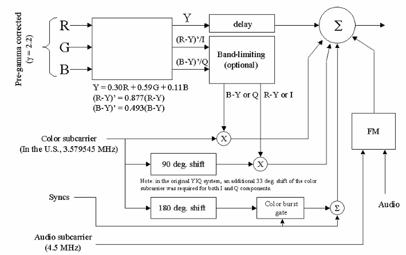
When a new signal is brought into a studio whether it is coming from a satellite receiver a camcorder or any other source the first thing to do is to synchronize it with the rest of the signals in the studio using a genlock circuit. The block diagram of pal encoder is shown in figure it uses the gamma corrected rgb signals from the camera tube as input and produces the composite colour video signal at its output. Page 46 block diagram 1. The gamma corrected rgb signals are applied to the y matrix which is a resistive network.
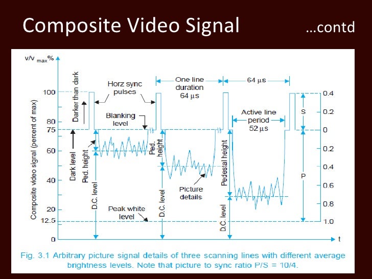
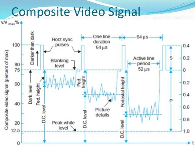
The blanking pulses of the composite video signal drive the picture tube beyond. Composite video signal 2 composite video signal fig 12 2 13. Luminance color difference to composite video conversion methods. This monitor was used with cga video interface cards and operated with a horizontal scan frequency of 15 75 khz and a vertical scan frequency of 60 hz.
A typical block diagram of a composite mono video. The composite signal in equation 4 8 consists of three sinusoids with frequencies f 1 hz f 2 hz f 3 hz and amplitudes a 1 a 2 a 3 respectively. Overall block diagram cvbs 3 21. Figure 1shows a block diagram for a genlock which takes an sdi serial.
The block diagram of a system is shown in the figure. The sound signal is separately detected demodulated and amplified before feeding it to the loudspeaker. Composite video signal consist of camera signal corresponding to the desired picture information blanking pulses to make the retrace invisible synchronizing pulses to synchronize the transmitter and receiver scanning horizontal sync pulse vertical sync pulse their amplitudes are kept same but their duration are. It is based on a sampling frequency of 7500 hz with the number of samples being 400.

Video Systems And Monitors

Video Test Pattern Generator Pattern Cum Sound Signal Generator

Cn0264 Circuit Note Analog Devices
Standards For Analog Video Part I Television Display Interfaces Part 1
Epanorama Net Links

Diagram Wiring Diagram Vga Toposite Full Version Hd Quality Vga Toposite Thediagramlibrary K Danse Fr

Ntsc Decoding
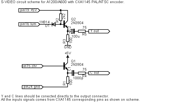
S Video In A1200 A600
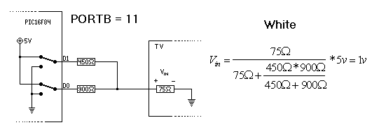
How To Generate Video Signals In Software Using A Pic

Block Diagram Of Television Transmitter

Video Signal An Overview Sciencedirect Topics

Block Diagram Of The Electronic Subsystems The Star Camera Computer Download Scientific Diagram

Digital Transmitter An Overview Sciencedirect Topics


